Lam Research CEO Says AI Demand for Fast SLC NAND in XL Flash and High Bandwidth Flash Could Tighten Global NAND Wafer Supply

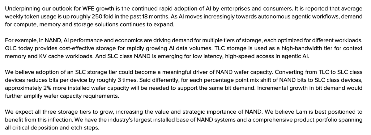
Arguably the most valuable insight from the past few days of memory industry news came from Lam Research CEO Tim Archer. On the company’s October 21, 2026 earnings call, Archer explained that the growing adoption of SLC NAND for AI could increase the wafer capacity needed to supply the same amount of storage. Let’s take a closer look. Specifically, moving from TLC to SLC-class products reduces the number of bits stored per cell to roughly one-third. As a result, he said, every 1-percentage-point increase in SLC’s share of total NAND bits would require approximately 2% more wafer capacity to meet the same overall bit demand. Some readers may wonder whether SLC is an outdated approach to NAND production, used mainly in legacy products. Far from it. SLC is a highly promising area that could play a role in NAND similar to the one HBM plays in DRAM. NAND customers, including NVIDIA and the hyperscalers, are developing next-generation products based on SLC. Within the NVIDIA ecosystem, the focus is on SLC-based XL-Flash, also known as high-IOPS NAND. Outside the NVIDIA ecosystem, SLC is also being used as the basis for HBF. Put simply, matching the storage capacity of one TLC wafer requires roughly three SLC wafers, while matching one QLC wafer requires roughly four. As production of these SLC-based products ramps up, they will consume an increasing amount of NAND wafer capacity. Just as HBM drove shortages in DRAM, these products could create a similar dynamic in NAND. With HBF and XL-Flash scheduled to enter volume production in 2028 and 2027, respectively, I think we should consider whether some analysts’ forecasts of NAND prices beginning to decline in the fourth quarter of 2027 may be overly conservative.
Context
Converting triple level or quad level flash wafers into single level cell NAND for ultra fast AI storage sacrifices two thirds to three quarters of bit capacity per wafer, threatening an HBM style supply crunch across the flash memory market.
As AI context windows and key value caches grow beyond what DRAM and HBM can hold economically, hardware architects are turning to ultra low latency single level cell (SLC) NAND flash to build a fast intermediate memory tier.
Deep dive
Semiconductor analyst Jukan highlighted remarks on Monday morning from Lam Research chief executive Tim Archer explaining that rising AI adoption of single level cell (SLC) NAND flash could trigger a wafer capacity squeeze in the flash storage market similar to the squeeze High Bandwidth Memory caused in DRAM.
Because SLC NAND stores only one bit per memory cell compared with three bits in standard TLC flash and four bits in QLC flash, matching the storage capacity of a single TLC wafer requires roughly three SLC wafers. Archer noted on Lam Research's earnings call that every 1 percentage point increase in SLC's share of total NAND bits requires approximately 2 percent more global wafer capacity to deliver the same total storage volume.
Nvidia and major cloud hyperscalers are actively developing SLC based architectures for AI clusters, including high IOPS XL Flash slated for volume production in 2027 inside the Nvidia ecosystem and High Bandwidth Flash (HBF) targeted for 2028.
What to expect next
Flash memory manufacturers Kioxia, Samsung, SK hynix, and Micron will weigh capital equipment orders with suppliers like Lam Research as XL Flash and HBF ramps absorb NAND wafer supply in 2027 and 2028.Industry analysts expect concrete adoption milestones to emerge over the coming quarters as initial deployments scale across production environments. Enterprise storage buyers and cloud architects planning 2027 and 2028 cluster deployments may need to lock in long term NAND supply agreements early if SLC based AI flash products absorb a growing share of global wafer starts.