TSMC Will Reportedly Resume SRAM Bitcell Scaling on Its 1.4nm A14 Node, Shrinking 6T Cells Below 0.017 Square Micrometers

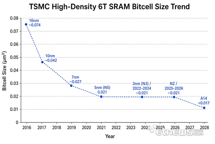
TSMC is finally set to resume SRAM scaling with its A14 node, following a stall that began after N5, according to Korean media reports. SRAM bitcell sizes have remained at 0.021 µm² for roughly eight years since the introduction of the N5 (5 nm) process in 2020. With A14, however, the size of a high-density 6T SRAM (static random-access memory) bitcell is expected to shrink to below 0.017 µm². Korean media noted that this would put TSMC ahead of Intel’s 18A process, for which Intel reported a high-density bitcell size of 0.021 µm² and a maximum SRAM macro density of 38.1 megabits/mm² at last year’s ISSCC. SRAM is the ultrafast cache memory used inside CPUs, GPUs, and AI accelerators. Smaller bitcells—the smallest individual memory cells—allow more memory to fit into the same area, directly affecting performance and power efficiency.
Context
Breaking an eight year stall in on chip SRAM cache density allows future AI accelerators and CPUs to pack significantly larger ultra fast local memory directly onto logic dies, reducing off chip HBM bottlenecks.
While logic transistors continued shrinking from 5 nanometer to 3 nanometer and 2 nanometer nodes, static random access memory (SRAM) bitcells stalled around 0.021 square micrometers due to quantum tunneling and FinFET layout limits.
Deep dive
TSMC is set to resume scaling down the physical size of static random access memory (SRAM) bitcells with its upcoming A14 (1.4 nanometer class) process node, ending an eight year plateau that began with the 5 nanometer N5 node in 2020, according to South Korean media reports summarized by Jukan on Monday.
Across N5, N3, and N2, high density six transistor (6T) SRAM bitcells remained stuck near 0.021 square micrometers, matching the 0.021 square micrometer bitcell reported by Intel for its 18A process at ISSCC. On A14, second generation nanosheet gate all around transistors enable TSMC to shrink the high density 6T SRAM bitcell below 0.017 square micrometers, a reduction of roughly 20 percent in cell area.
Because AI inference chips rely heavily on on die SRAM caches to hold activations and key value states close to tensor compute units, shrinking the SRAM bitcell directly boosts on chip cache capacity and energy efficiency.
What to expect next
AI chip designers planning 2028 and 2029 accelerators on TSMC's A14 node will use the higher SRAM density to expand L2 and scratchpad caches, reducing power hungry round trips to external HBM stacks.Industry analysts expect concrete adoption milestones to emerge over the coming quarters as initial deployments scale across production environments. Resuming SRAM scaling on A14 will also intensify foundry competition with Intel and Samsung as AI processor architects prioritize on die memory bandwidth and cache capacity per watt for reasoning workloads.